- 您现在的位置:买卖IC网 > Sheet目录3851 > PIC32MX130F064D-I/ML (Microchip Technology)IC MCU 32BIT 64KB FLASH 44-QFN
PIC32MX1XX/2XX
DS61168D-page 152
Preliminary
2011-2012 Microchip Technology Inc.
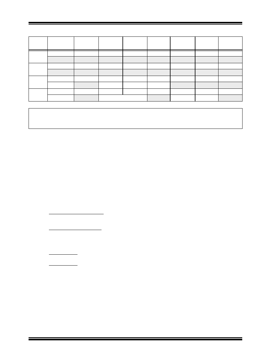
REGISTER 12-1:
T1CON: TYPE A TIMER CONTROL REGISTER
Bit
Range
Bit
31/23/15/7
Bit
30/22/14/6
Bit
29/21/13/5
Bit
28/20/12/4
Bit
27/19/11/3
Bit
26/18/10/2
Bit
25/17/9/1
Bit
24/16/8/0
31:24
U-0
—
23:16
U-0
—
15:8
R/W-0
U-0
R/W-0
R-0
U-0
ON(1)
—
SIDL
TWDIS
TWIP
—
7:0
R/W-0
U-0
R/W-0
U-0
R/W-0
U-0
TGATE
—
TCKPS<1:0>
—
TSYNC
TCS
—
Legend:
R = Readable bit
W = Writable bit
U = Unimplemented bit, read as ‘0’
-n = Value at POR
‘1’ = Bit is set
‘0’ = Bit is cleared
x = Bit is unknown
bit 31-16 Unimplemented: Read as ‘0’
bit 15
ON: Timer On bit(1)
1 = Timer is enabled
0 = Timer is disabled
bit 14
Unimplemented: Read as ‘0’
bit 13
SIDL: Stop in Idle Mode bit
1 = Discontinue operation when device enters Idle mode
0 = Continue operation even in Idle mode
bit 12
TWDIS: Asynchronous Timer Write Disable bit
1 = Writes to TMR1 are ignored until pending write operation completes
0 = Back-to-back writes are enabled (Legacy Asynchronous Timer functionality)
bit 11
TWIP: Asynchronous Timer Write in Progress bit
In Asynchronous Timer mode:
1 = Asynchronous write to TMR1 register in progress
0 = Asynchronous write to TMR1 register complete
In Synchronous Timer mode:
This bit is read as ‘0’.
bit 10-8
Unimplemented: Read as ‘0’
bit 7
TGATE: Timer Gated Time Accumulation Enable bit
When TCS = 1:
This bit is ignored.
When TCS = 0:
1 = Gated time accumulation is enabled
0 = Gated time accumulation is disabled
bit 6
Unimplemented: Read as ‘0’
bit 5-4
TCKPS<1:0>: Timer Input Clock Prescale Select bits
11 = 1:256 prescale value
10 = 1:64 prescale value
01 = 1:8 prescale value
00 = 1:1 prescale value
Note 1: When using 1:1 PBCmLK divisor, the user’s software should not read/write the peripheral SFRs in the
SYSCLK cycle immediately following the instruction that clears the module’s ON bit.
发布紧急采购,3分钟左右您将得到回复。
相关PDF资料
PIC18LF46K80-I/ML
MCU PIC ECAN 64KB FLASH 44QFN
AT89S51-24JI
IC 8051 MCU 4K FLASH 44PLCC
AT89S51-24JC
IC 8051 MCU 4K FLASH 44PLCC
AT89S51-24AI
IC 8051 MCU 4K FLASH 44TQFP
AT89S51-24AC
IC 8051 MCU 4K FLASH 44 TQFP
AT89LS52-16PI
IC 8051 MCU FLASH 8K 40DIP
AT89LS52-16PC
IC MCU 8K FLASH LV 16MHZ 40-DIP
AT89LS52-16JI
IC 8051 MCU FLASH 8K 44PLCC
相关代理商/技术参数
PIC32MX130F064D-I/PT
功能描述:32位微控制器 - MCU 32B MCU 64KB FL 16KB RAM 40MHz 44Pin
RoHS:否 制造商:Texas Instruments 核心:C28x 处理器系列:TMS320F28x 数据总线宽度:32 bit 最大时钟频率:90 MHz 程序存储器大小:64 KB 数据 RAM 大小:26 KB 片上 ADC:Yes 工作电源电压:2.97 V to 3.63 V 工作温度范围:- 40 C to + 105 C 封装 / 箱体:LQFP-80 安装风格:SMD/SMT
PIC32MX130F064D-I/TL
功能描述:32位微控制器 - MCU 32B MCU 64KB FL 16KB RAM 40MHz 44Pin
RoHS:否 制造商:Texas Instruments 核心:C28x 处理器系列:TMS320F28x 数据总线宽度:32 bit 最大时钟频率:90 MHz 程序存储器大小:64 KB 数据 RAM 大小:26 KB 片上 ADC:Yes 工作电源电压:2.97 V to 3.63 V 工作温度范围:- 40 C to + 105 C 封装 / 箱体:LQFP-80 安装风格:SMD/SMT
PIC32MX130F064DT-I/ML
功能描述:32位微控制器 - MCU 32B MCU 64KB FL 16KB RAM 40MHz 44Pin
RoHS:否 制造商:Texas Instruments 核心:C28x 处理器系列:TMS320F28x 数据总线宽度:32 bit 最大时钟频率:90 MHz 程序存储器大小:64 KB 数据 RAM 大小:26 KB 片上 ADC:Yes 工作电源电压:2.97 V to 3.63 V 工作温度范围:- 40 C to + 105 C 封装 / 箱体:LQFP-80 安装风格:SMD/SMT
PIC32MX130F064DT-I/PT
功能描述:32位微控制器 - MCU 32B MCU 64KB FL 16KB RAM 40MHz 44Pin
RoHS:否 制造商:Texas Instruments 核心:C28x 处理器系列:TMS320F28x 数据总线宽度:32 bit 最大时钟频率:90 MHz 程序存储器大小:64 KB 数据 RAM 大小:26 KB 片上 ADC:Yes 工作电源电压:2.97 V to 3.63 V 工作温度范围:- 40 C to + 105 C 封装 / 箱体:LQFP-80 安装风格:SMD/SMT
PIC32MX130F064DT-I/TL
功能描述:32位微控制器 - MCU 32B MCU 64KB FL 16KB RAM 40MHz 44Pin
RoHS:否 制造商:Texas Instruments 核心:C28x 处理器系列:TMS320F28x 数据总线宽度:32 bit 最大时钟频率:90 MHz 程序存储器大小:64 KB 数据 RAM 大小:26 KB 片上 ADC:Yes 工作电源电压:2.97 V to 3.63 V 工作温度范围:- 40 C to + 105 C 封装 / 箱体:LQFP-80 安装风格:SMD/SMT
PIC32MX130F064DT-V/ML
功能描述:32位微控制器 - MCU 32B MCU 64KB FL 16KB RAM 40MHz 44Pin
RoHS:否 制造商:Texas Instruments 核心:C28x 处理器系列:TMS320F28x 数据总线宽度:32 bit 最大时钟频率:90 MHz 程序存储器大小:64 KB 数据 RAM 大小:26 KB 片上 ADC:Yes 工作电源电压:2.97 V to 3.63 V 工作温度范围:- 40 C to + 105 C 封装 / 箱体:LQFP-80 安装风格:SMD/SMT
PIC32MX130F064DT-V/PT
功能描述:32位微控制器 - MCU 32B MCU 64KB FL 16KB RAM 40MHz 44Pin
RoHS:否 制造商:Texas Instruments 核心:C28x 处理器系列:TMS320F28x 数据总线宽度:32 bit 最大时钟频率:90 MHz 程序存储器大小:64 KB 数据 RAM 大小:26 KB 片上 ADC:Yes 工作电源电压:2.97 V to 3.63 V 工作温度范围:- 40 C to + 105 C 封装 / 箱体:LQFP-80 安装风格:SMD/SMT
PIC32MX130F064DT-V/TL
功能描述:32位微控制器 - MCU 32B MCU 64KB FL 16KB RAM 40MHz 44Pin
RoHS:否 制造商:Texas Instruments 核心:C28x 处理器系列:TMS320F28x 数据总线宽度:32 bit 最大时钟频率:90 MHz 程序存储器大小:64 KB 数据 RAM 大小:26 KB 片上 ADC:Yes 工作电源电压:2.97 V to 3.63 V 工作温度范围:- 40 C to + 105 C 封装 / 箱体:LQFP-80 安装风格:SMD/SMT